物理研究所,中国科学院发现了具有超伴随的透
时间:2025-06-04 10:27 作者:BET356官网在线登录
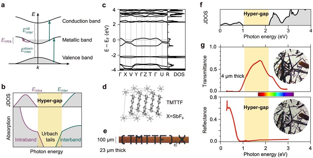
6月2日的Home报告说,根据中国科学学院的官方网站,透明的导体既具有电导率和透明度,又广泛用于触摸屏,太阳能电池,发光二极管,电动色素和透明的表现,并成为现代现代信息和技术中的必要材料。目前,主要的透明导体源自原始透明带隙材料(半导体或绝缘体)。掺杂过程以部分透明度为代价达到了电导率,并实现了电导率和光传输之间的平衡。为了打破这一限制,20年前(2005年)提出了一种固有的透明导体概念,不需要掺杂,以通过非常特殊的能量结构实现完美的透明度,但直到今天在实际材料中都没有发现。最近,来自中国ACA研究所的医生Wu Zhengran科学疾病/光体物理学的主要实验室,北京国家凝结物理学研究中心,以及更多在研究人员的指导下,在研究人员的指导下,第一次发现了这种内在的透明金属。 -absorbent band between the absorption of intraband and the absorption of the intensify It requires that its metal band get rid ofy that is enough, and the metal bandwidth is smaller than the energy difference between the Fermi surface and other covered states and non -conquered states, so that the absorption caused by the intraband transition can be cut down by metal bandwidth bandwidth, and the Cutoff energy that absorbs this band is smaller than the initial energy在频带之间吸收框架,a,b)这样的金属超伴侣,研究小组的Hu Xiaolei博士曾经使用完整的非有机数据库材料进行了高通量搜索。 PHY。 Rev. 6,065203(2022)的材料,但在实际系统中发现,大多数材料不是导电实验。 ▲图:理论原理,材料预言和实验发现超伴侣透明导体。研究团队没有放弃。 In the latest task, they calculated and found that a class of well -known organic conductors, TMTTF2X, could meet the conditions of the hyperbandgap (picture C, D), and enlarged the sample with electrochemical crystals (photo E), and the bulk single crystal showed a significant transparent window in the predicted Hyperboardgap band (photo f, g)) Destroying from visible red lights nearby that still do not send light to the light that is about to生长30微米。最低的光损耗(投机的介电函数)约为0.01,这是最低O的值f众所周知的化学计量金属,以及在商业透明的导电氧化物膜中(此),而其传播和改进却小于它。这项工作实验首次将电子电导率和光学透明度与固有固体材料相结合,开辟了一条新的路径,以实现通过超基色的透明电导率。相关的结果以“超间隙透明指挥”为标题发表在自然自然杂志上。 Sciencessi Wu Zhengran的中国学院是第一个设定了物理学研究所的L01小组的医生,SC08组的副研究人员Li Chunhong帮助了样本。 Hu Xiaolei是L01小组的毕业生,学生Chen Kun,Guo Xiang和Postdoctoral Li Yan都参加了这项工作。相应的论文是研究人员lu ling。该研究由中国国家自然科学基金会和中国科学院资助加密。


